An Afternoon with SMT, TRIM, and SMART
First Published: 23/02/25
And I entered graduate school. The first course I took was in computer graphics.
It was a brand new program. There were no textbooks. So Ivan Sutherland taught it -- there was Ron Resch… I didn’t know who these guys were. Ivan Sutherland came in, he was wearing flip flops, and I thought it was one of the hippie graduate students that was teaching the course. I didn't know.
I knew nothing. I walked into that class, I didn't know who those teachers were. This was just a course that sounded interesting. So I started to take this class, and we were asked to use this rather crude program they had for making pictures with spheres and elliptical objects, or if we wanted we could write our own code to do something. Well, screw using that existing package,--- I wanted to write my own stuff. And I was completely pulled into it.
One of the things I did there was I made a model of my left hand. I digitized it. In fact, the way I made the model was--- I put my hand in plaster of Paris, and that's where I discovered you need to put Vaseline on the back of your hand, which I didn't know at the time. So, my hand got stuck in the mold. Stuck a knife down in there to cut my hand out of that. And then went through this laborious process of digitizing, and then I wrote a program to animate it, and then that led to getting my first paper published in the ACM in Boston--- in 1972, I think is when it was.
- Ed Catmull, describing one of his first graduate projects in his oral history.
After using my 2015 13-inch MacBook Air for quite a few years, I finally took the plunge and got myself a new laptop. To call my older boyo’s specs a bit dated would be an understatement. The now-veteran ran on a processor from Intel's Broadwell series — a dual-core i5-5250U with a base clock speed of 1.6 GHz, which could turbo boost up to 2.7 GHz. Thanks to hyper-threading, each physical core could handle two threads simultaneously, effectively acting as four logical CPUs. It had two memory slots, each containing a 4 GB RAM module. This was a 1600 MHz DDR3 manufactured by Hynix. However, the icing on the cake was its 256 GB PCIe-based SSD, a significant upgrade over the previous generation’s SATA-based SSDs. This one had a four-lane PCIe connection with a transfer speed of 5 GT/s per lane — so likely PCIe 2.0!
Now, some of you might be wondering — how can one survive with a 256 GB SSD for 5+ years? The answer is: on a wing and a prayer. On a serious note, the low storage never bothered me one iota. As of yesterday, I still had around 86 GB available. Most of my space is taken up by a trifecta of code, documents, and images anyway. As the saying goes, data expands to fill the space available for storage.
Tangentially, if you want to find this hardware information on macOS,
you can simply use system_profiler -detailLevel basic along
with some good ol’ grep -A 20 commands.
When purchasing my new laptop, I was kind of tempted to go the “Windows on ARM” route with their new Surface lineup, which has excited me a great deal last year. However, after some careful deliberation, I decided to give it two more years — hoping for a little more stable x86 translation experience. For now, I have somewhat settled on a 2023 MacBook Pro loaded up with their M2 Pro chip. This new recruit brings with it 16 GB of LPDDR5 RAM from Micron and, this time around, a whopping 1 TB PCIe-based NVMe SSD soldered to the motherboard.
SMT
Now, I really would have preferred removable SSDs, but that train's been long gone. The manufacturer incentive seems too strong of a pull for them to budge. Integrated SSDs allow for a more compact and lighter form factor, simplify assembly, and lower manufacturing costs. As I understand it, they achieve this using surface-mount technology (SMT). Paul Vianco, currently at Sandia, wrote a nice book chapter in 2001 describing SMT from a broader perspective:
Since the 1980s there has been a significant growth in the use of surface mount technology for electronics assembly. The advantages of surface mount include reduced board size through denser circuitry, lower product weight through device miniaturization, simplified circuit board fabrication with the absence of holes, and faster circuitry because package leads and long signal traces are eliminated. Also, large-volume, surface mount assembly processes can produce high-quality consumer and military electronics in a cost-effective manner.
As the term implies, surface mount technology uses electronic devices that are soldered only to the surface of the circuit board. Packages may have leads along two or all four sides of their periphery. Lead configurations include the gull-wing lead, J-lead, and S-lead geometries. Some packages have no leads at all. So-called leadless discrete devices include discrete resistors, capacitors, and inductors. The solder connection is made to a conductive surface or termination made from a fired-on metal film (typically silver-based with a nickel or copper barrier layer). Silicon chips are mounted in larger, leadless packages termed leadless ceramic chip carriers (or LCCCs). The solder connection is made to a conductive surface referred to as the castellation, which is also comprised of a fired-on metal coating (typically gold).
There is also an interesting article from Steve Burke at GamersNexus from about a decade ago, explaining how RAM and SSDs are made at Kingston’s SMT lines. Today, many surface-mount packaging technologies are used to attach these ICs to circuit boards.
From what I can tell, the packaging technology used for SSD components is Ball Grid Array (BGA). In BGA, components are mounted onto the SSD using an array of solder balls. Because these tiny solder balls are arranged in a grid pattern instead of just along the edges, they allow for a large number of I/O connections in a small space — providing high density. This naturally helps more data transfer simultaneously in a small form factor. Also, because the solder balls are in direct contact with the circuit board, heat generated by the chip is transferred away efficiently — providing high heat conduction. Again, this can help extend the lifespan of SSDs, as mentioned in this StackExchange post:
However, studies like the one Facebook conducted in their own data centers found that the hotter your SSD runs, the quicker it wears out the flash memory inside of the drive. So while an SSD can technically operate at the higher ranges advertised by manufacturers, you’re going to get better data integrity and more life out of your SSD if you keep it cool.
The Wikipedia page also discusses how BGAs seem to provide low-inductance leads, which is quite advantageous. Inductance is "the tendency of an electrical conductor to oppose a change in the electric current flowing through it". Therefore, low-inductance leads allow electrical conductors (solder balls in BGA) to have minimal resistance to fast-changing currents. From an SSD point of view, this can allow quicker and more stable data transfer.
As I am sure we can agree, these factors are quite attractive for manufacturing mass-produced consumer electronics, which is why we seem to have boarded the "bye-bye removable SSDs" train! Whoa, what a tangent this was!
TRIM
Circling back to my new laptop, when I was comparing its specs with my older machine, I noticed something fun — both had the following statement in their SSD configs: "TRIM Support: Yes". Now, I was not quite sure what TRIM meant, so I started digging into it, and boy, was it fascinating! Two of the most concise insights I found were from Brendan Gregg’s System Performance book and Louis Gerbarg’s 2009 blog post on SSDs.
You see, there are standard interfaces used for connecting HDDs and SSDs to computers. For instance, there is SATA (Serial ATA), SCSI, and NVMe over PCIe. The ATA implementation standard consists of an ATA/ATAPI Command Set that specifies the collection of command sets a host system can use to access storage devices. One of these is the ATA TRIM command. Brendan Gregg succinctly describes this in his book:
it informs the SSD that a region is no longer in use, allowing the SSD to more easily assemble its pool of free blocks, reducing write amplification. (For SCSI, this can be implemented using the UNMAP or WRITE SAME commands; for ATA, the DATA SET MANAGEMENT command. Linux support includes the discard mount option, and the fstrim(8) command.)
Let us break this down by first understanding SSD internals at a glance. Tyler Bletsch’s Enterprise Storage Architecture slides from Duke include a great summary picture of SSD internals.
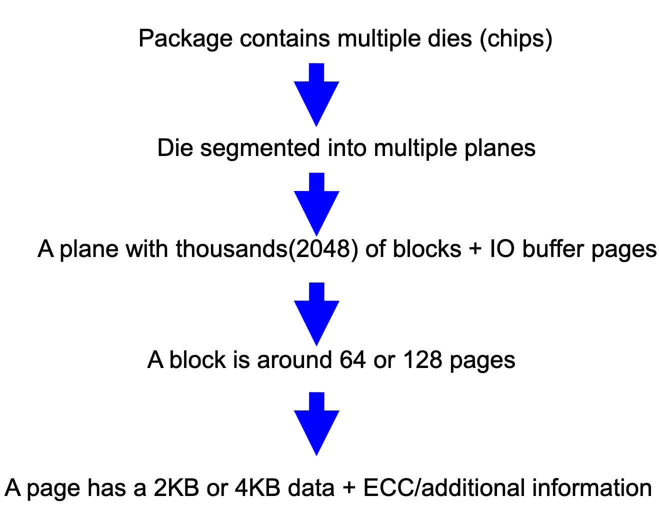
This chart is fantastically expanded upon by Hu et al. in their 2011 ICS paper on SSD performance optimization:
To increase storage density, flash manufactories package several flash chips together, a model called package. All chips in a package share the same 8/16-bit I/O bus of the package but have separate chip enable and ready/busy control signals. Each chip is composed of two or more dies. Each die has one internal ready/busy signal that is different from the external ready/busy signal of a chip. The internal ready/busy signal is invisible to user. It will only be used in advanced commands. Each die is composed of multiple planes. Each plane contains thousands of flash blocks and one or two data/cache registers used as an I/O buffer. A flash block typically consists of 64 or 128 pages, where a page is further divided into many 512B sub-pages. Each sub-page has a 16B spare space used to store a variety of information, such as error correction code (ECC), logical page number and sub-page state. The size of a page has been steadily increasing due to the technology development as well as the growing size of a single chip. While chip and die are not clearly distinguished and often confused with each other in many previous studies in the literature, chip enable and read/busy signals make them clearly distinct from each other. A chip is the basic functional unit that has its independent chip enable and read/busy signals. A die is a component of a chip, which only has an internal read/busy signal.
This dissection from 2011 remains largely true today. For instance, here is a specification of Samsung’s SZ1735a Z-SSD, used in data centers. Additionally, here is its product brief. While a page may contain sub-pages, modern SSD specs seem to refer only to the whole page size instead. For instance, we can infer SZ1735a’s page size by looking at the “Data I/O Speed” section, which describes a 4KB data size. Block sizes are not typically mentioned either, but if we consider a typical range of 128 to 512 pages, we are looking at blocks with sizes around 512KB (128 pages x 4KB) to 2048KB (512 pages x 4KB).
So how is all of this related to the TRIM command? What you just witnessed was a Pledge. Now, here is the Turn:
An SSD write operation can be done to a single page but, due to hardware limitations, erase commands always affect entire blocks; consequently, writing data to empty pages on an SSD is very fast, but slows down considerably once previously written pages need to be overwritten. Since an erase of the cells in the page is needed before it can be written to again, but only entire blocks can be erased, an overwrite will initiate a read-erase-modify-write cycle: the contents of the entire block are stored in cache, then the entire block is erased from the SSD, then the overwritten page(s) is written into the cached block, and only then can the entire updated block be written to the flash medium. This phenomenon is known as write amplification.
So what is this "hardware limitation" that Wikipedia is referring to? Western Digital’s 2018 whitepaper on flash perfectly describes this limitation:
The basic NAND flash cell is a floating gate transistor with the bit value determined by the amount of charge trapped in the floating gate. NAND flash uses tunnel injection for writing/programming and tunnel release for erasing the cell.
In SLC (Single-Level Cell):
- Writing (e.g., programming) to a cell causes the accumulation of negative charge in the floating gate, resulting in a “0” bit value for that cell.
- Erasing a cell removes the negative charge in the floating gate, resulting in a “1” bit value for that cell. To change the bit content of a cell from “0” to “1”, the cell must be erased. Due to the NAND architecture of sharing bit control lines and word control lines across multiple storage transistors, erasing a cell requires erasing the entire Erase Block, which contains that cell.
What Western Digital is explaining in their whitepaper is that this design is geared toward simplicity and density, which, in turn, keeps costs down. While allowing for selective erasure of individual pages might be theoretically possible, it would likely require adding more complex circuitry. This would increase costs by potentially reducing the storage density of the chips and increasing the physical size of each die.
And now for the Prestige. How would you do it — mitigate write amplification? A natural thought would be to hold off on performing an erasure. When data needs to be updated, start by writing the updated data to an empty page. Next, mark the old page containing outdated data as invalid. Finally, keep track of valid and invalid pages. When the SSD needs more space or when the system is idle, the block containing invalid pages can be erased in a garbage collection process. This avoids a costly read-erase-modify-write cycle.
And that is how SSDs mitigate write amplification. The tracking of valid and invalid pages is handled by the SSD’s controller using the Flash Translation Layer (FTL) component. The TRIM command, in turn, is sent by the OS to inform the SSD controller which blocks or pages of data are invalid and no longer needed by the OS. This helps the FTL update its mapping table and later perform a cleanup during the garbage collection process. Here is a 2009 whitepaper from Intel summarizing this:
Unlike traditional hard disk drives, it is advantageous to tell an SSD when you delete files. At some point every 4KB page has been written to once, and you have to start overwriting old existing data. Unlike spinning media, Flash media can not simply overwrite existing data and must first perform a 512KB block erase. To overwrite existing data, an SSD requires a longer read-modify-write operation which is the basis for slowing write performance as the drive fills.
Previously, there was no ATA command that would physically erase user-deleted data from a storage device. The Intel® SSD Optimizer takes advantage of the new DATA SET MANAGEMENT command now available in the ATA8-ACS-2 specification. A feature of this new command is known as “Trim”, which allows the host to collect file system information from the OS and proactively send it to the drive. By knowing which files are no longer valid, the drive can better manage its operations.
Furthermore, much of what I have described here has been thoroughly examined in FlashDBA’s blog posts. I highly encourage you to check out his posts on understanding blocks, pages, and program/erase cycles; understanding SLC, MLC, and TLC; and exploring FTL.
This would be a good time to scroll back up and revisit Brendan Gregg’s summary on TRIM. Give yourself a homecoming, if you will!
SMART
The rabbits might be wondering whether I am done with SSDs, and if so, can we now move on to greener pastures? Well, hoppity-hop... not just yet! You see, when I was exploring the SSD configs, another setting caught my attention — "S.M.A.R.T. status: Verified". So, I thought about doing a "Mr. Beanish" dive into SMART as well.
SMART stands for Self-Monitoring, Analysis, and Reporting Technology and is a "signaling method between sensors in the drive and the host computer". It helps the host monitor the drives to assess their health and reliability. The "Verified" status above indicates that my SSD’s monitoring system has found everything to be hunky-dory. Samsung, in a 2014 application note, describes this in greater detail:
S.M.A.R.T. monitors computer drives to detect and report on various reliability indicators. The technology aims to anticipate failures and warn users of impending drive failure, allowing the user to replace an ailing drive to avoid data loss and/or unexpected outages. Of course, SMART can only warn of predictable errors, which result from slow processes like mechanical wear and can be predicted by analyzing certain indicators (such mechanical problems accounted for 60% of HDD failures). Unpredictable failures, like a sudden mechanical failure resulting from an electrical surge, have no measurable variables to track and analyze. Modern SMART implementations (in HDDs) also try to prevent failures by attempting to detect and repair sector errors. All data and all sectors are tested to confirm the drive’s health during periods of inactivity.
..... it is important to remember that SMART attributes vary in both meaning and interpretation by manufacturer. Some attributes are considered trade secrets, and not all drives report the same SMART attributes.
The same document goes on to describe various attributes supported by Samsung’s then monitoring systems. The most important one seems to be the "Reallocated Sector Count" attribute:
The raw value of this attribute represents the number of sectors that have been moved as a result of a read error, write error, or a verification error. If the firmware detects any of these types of errors, all valid data in the block the error originates from must be transferred to a new block. This number should be low because a high number would indicate a large number of failures.
Another important attribute might be the "Wear Leveling Count". It represents the number of times a block has been erased. This directly relates to the SSD's lifespan, as each NAND flash cell can only be erased and rewritten a finite number of times before eventually wearing out. For instance, the SZ1735 specification we looked at earlier has a dedicated section on reliability.
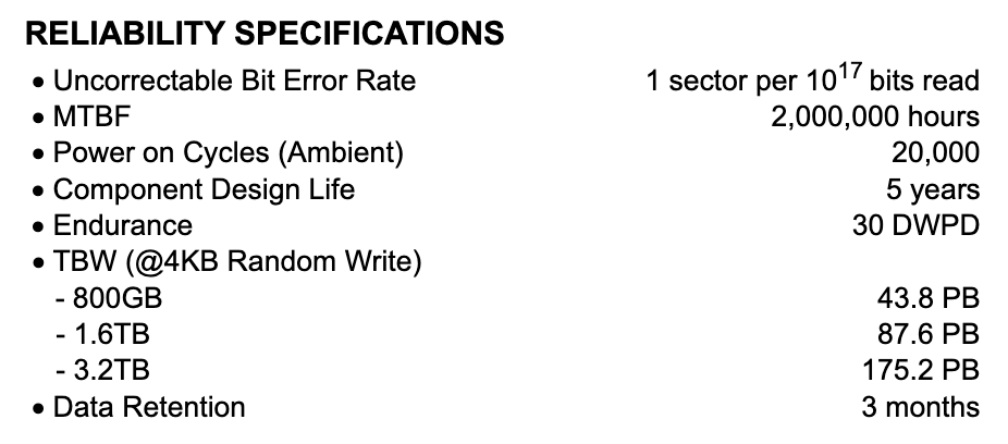
To elaborate on these specs, the 30 DWPD endurance means that we can perform 30 drive writes per day over the component design life (i.e., the warranty) of five years. In other words, we can overwrite the drive’s entire capacity each day for five years. Similarly, the TBW (Total Bytes Written) represents the total amount of data that can be written to the drive during its lifetime. Although the specs mention this for us, we can trivially calculate it ourselves using the DWPD number, drive size, and warranty period. For an 800GB SSD with 30 DWPD endurance and a 5 year warranty period, we get a TBW of 5 x 365 x 800 x 30 = 43,800,000 GB or 43.8 PB.
For Wear Leveling Counts, we need to figure out the average number of erasure cycles on SSD blocks. This can be a bit nuanced, as it also depends on the NAND cell technology — whether it's SLC, MLC, etc. Anyway, how do we find the SMART attributes that my current MacBook supports?
Well, we can simply run a
brew install smartmontools followed by
smartctl -a disk0. This fetches the information. Here is
what I see on my Macbook Pro:
=== START OF INFORMATION SECTION ===
Model Number:                   		APPLE SSD AP1024Z
Serial Number:                  		<REDACTED>
Firmware Version:               		<REDACTED>
PCI Vendor/Subsystem ID:        		0x106b
IEEE OUI Identifier:            		0x000000
Controller ID:                  		0
NVMe Version:                   		<1.2
Number of Namespaces:           		3
Local Time is:                  		Sun Oct 20 18:42:57 2024 EDT
Firmware Updates (0x02):        		1 Slot
Optional Admin Commands (0x0004):       Frmw_DL
Optional NVM Commands (0x0004): 		DS_Mngmt
Maximum Data Transfer Size:     		256 Pages

Supported Power States
St Op 	Max   Active 	Idle   RL RT WL WT  Ent_Lat  Ex_Lat
 0 + 	0.00W   	-    	-	0  0  0  0    	0   	0

=== START OF SMART DATA SECTION ===
SMART overall-health self-assessment test result: PASSED

SMART/Health Information (NVMe Log 0x02)
Critical Warning:               	0x00
Temperature:                    	33 Celsius
Available Spare:                	100%
Available Spare Threshold:      	99%
Percentage Used:                	0%
Data Units Read:                	881,404 [451 GB]
Data Units Written:             	940,860 [481 GB]
Host Read Commands:             	16,193,127
Host Write Commands:            	8,627,677
Controller Busy Time:           	0
Power Cycles:                   	97
Power On Hours:                 	9
Unsafe Shutdowns:               	4
Media and Data Integrity Errors:	0
Error Information Log Entries:  	0

Read 1 entries from Error Information Log failed: GetLogPage failed: system=0x38, sub=0x0, code=745
As you can see, the attributes vary quite a bit. For instance, there is no wear leveling count. SSDs tend to reserve spare blocks to replace bad ones over time, so having 100% available spare means that all of my spare blocks are still intact. The "Data Units Written" probably indicates the total amount of data written to the SSD. The final message about the read entries from the error information log failing is likely because the SSD hasn't encountered any significant errors yet. Oh well!
Finally, I will end this discussion on SMART by pointing out the advice Brendan Gregg shared in his book:
While this is very useful, it does not have the resolution to answer questions about individual slow disk I/O, as kernel tracing frameworks do. The corrected errors information should be useful for monitoring, to help predict disk failure before it happens, as well as to confirm that a disk has failed or is failing.
Which makes sense to me. If performance diagnostics are what we are after, then maybe perf or ftrace is the way to go. Nevertheless, it is a pretty neat long-term monitoring technology, which I am sure many data centers heavily rely on.
Conclusion
With all these discussions on SMT, TRIM, and SMART, I kind of forgot to talk about the one thing I was bubbling to geek out on! You see, whenever we get a new system, our first instinct is to decide how we are going to baptize it.
Having a minimalistic taste, for me, this involved starting with a Firefox installation and setting up my favorite addons. This included my very own Popup Encyclopedia. Next, I imported my precious bookmarks, my password manager, and signed in to my online accounts. Once I was done removing the clutter from the dock and transferring my personal files, there were only three things left to take care of: iTerm2/Homebrew, VS Code, and UTM.
My iTerm2 customizations are really quite simple. All I do is:
- Enable “Copy to pasteboard on selection”
- Switch to the “GitHub Dark” ANSI color theme with dark mode editing
-
Keep transparency at 30% — you can switch to an opaque background
using
cmd + U -
Ensure that timestamps are always shown on the right —
shift + cmd + E. This is quite handy when logging something. - Switch to 10,000 scrollback lines
- Install the JetBrains Mono font
This was followed by importing my .zshrc configs. Over the
years, some nuggets I have curated in it are:
# For finding space consuming files and directories
alias spaceG='du -sh *  | grep -E "\dG" | sort -snr -k 1,1'
alias spaceM='du -sh *  | grep -E "\dM" | sort -snr -k 1,1'
alias tv='cd ~/parth/yt-shows/ && cd "$(ls | sort -R | tail -1)" && cd "$(ls | sort -R | tail -1)" && vlc "$(ls ./*.mp4 ./*.mkv | sort -R | tail -1)"'
alias download_album='yt-dlp --extract-audio --add-metadata --embed-thumbnail --audio-format mp3 -o "%(title)s.%(ext)s" --postprocessor-args "-id3v2_version 3"'
# My Bash prompt has remained the same in the past 8 years - a simple “time with seconds” and “current working dir”
PROMPT='[%*][%1d] '
Having UTM is quite handy for testing things out on Windows and Linux. Presently, I have configured an ARM-based Debian VM without a desktop environment. Next, my plan is to experiment with UTM + Windows 11.
And that's it, folks! Hope this was a fun dive! Until next time — happy exploring!
←